Wafer bonded cmuts can be fabricated by fusion bonding a silicon and a silicon on insulator soi wafers fig.
Wafer bonding for silicon on insulator technologies.
For all practical purposes the soi film thickness varies in mems applications from 4 to 200 μm.
The proposed bonding mechanism is polymerization of.
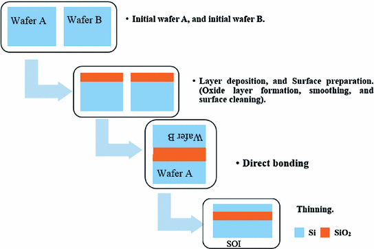
Silicon on insulator soi wafers are manufactured by bonding one si wafer to the other by activating the surface of both wafers and then placing them together so that a strong bond occurs first through the van der waals attraction and then by forming a covalent bond 59 activation of the superclean si surface is the key to accomplish this bonding typically by a remote plasma process.
Silicon on insulator soi is a semiconductor structure consisting of a layer of single crystalline silicon separated from the bulk substrate by a thin layer of insulator.
30 a thin sacrificial layer for example a sige layer is grown epitaxially on the initial donor wafer.
Precise and uniform cavity depth and high surface quality can easily be achieved by the well defined thermal oxidation process.
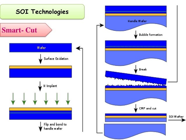
First developed in order to obtain soi wafers with very thin top silicon layers these techniques are referred to as bond and etch back silicon on insulator processes besoi.
In soi wafers the insulator is almost invariably a thermal silicon oxide sio 2 layer and the substrate is a silicon wafer.
It is proposed the wafers are drawn into intimate contact as a result of the gaseous oxygen between them being consumed by oxidation thus producing a partial vacuum.
A silicon wafer bonding process is described in which only thermally grown oxide is present between wafer pairs.
Specific techniques have been developed to achieve very thin layers through bonding and thinning processes.
The surface state of a silicon wafer can be measured by the contact angle a drop of water forms.
Sonix wafer inspection systems provide nondestructive testing ndt to detect gaps and voids of less than 0 1 micron enabling superior diagnostic imaging for wafer bonding and device level bond rings in silicon on insulator anodic metal to metal and other high end bonded wafer applications.
Defects can be precisely mapped as part of the.
It is proposed the wafers are drawn into intimate contact as a result of the gaseous oxygen between them being consumed by oxidation thus producing a partial vacuum.
Wafer bonding the insulating layer is formed by directly bonding oxidized silicon with a second substrate.
Depending on the type of application the.
7 3 shows a sampling of silicon film and buried oxide thicknesses based on a large number of soi wafer specifications for mems applications.
Bonding occurs after insertion into an oxidizing ambient.
The proposed bonding mechanism is polymerization of.
The majority of the second substrate is subsequently.
The cavity is formed by wet etching the thermally grown sio 2 layer on top of the silicon substrate.
Soi wafers for mems are nearly always fabricated by wafer bonding.
Direct bonding is mostly referred to as bonding with silicon.
Sio 2 based soi wafers can be produced by several methods.
Simox separation by implantation of oxygen uses an oxygen ion beam implantation process followed by high temperature annealing to create a buried sio 2 layer.